


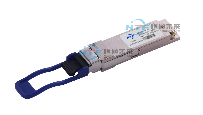
100Gb/s QSFP28 ER4 Optical Transceiver Module
It has to be noted that the operation in excess of any individual absolute maximum ratings might cause permanent damage to this module.
|
Parameter |
Symbol |
Min |
Max |
Unit |
Notes |
|
Storage Temperature |
TS |
-40 |
85 |
oC |
|
|
Power Supply Voltage |
VCC |
-0.3 |
4.0 |
V |
|
|
Relative Humidity (non-condensation) |
RH |
0 |
85 |
% |
|
|
Damage Threshold |
THd |
-3.0 |
|
dBm |
|
The following optical characteristics are defined over the Recommended Operating Environment unless otherwise specified.
|
Parameter |
Symbol |
Min. |
Typical |
Max |
Unit |
Notes |
|
|
Tran***itter |
|||||||
|
Lane w***elength(range) |
L0 |
1294.53 |
1295.56 |
1296.59 |
nm |
|
|
|
L1 |
1299.02 |
1300.05 |
1301.09 |
nm |
|
||
|
L2 |
1303.54 |
1304.58 |
1305.63 |
nm |
|
||
|
L3 |
1308.09 |
1309.14 |
1310.09 |
nm |
|
||
|
Signaling rate, each lane |
|
|
25.78125 |
|
GBd |
|
|
|
Side-mode suppression ratio |
***SR |
30 |
|
|
|
|
|
|
Total launch power |
PT |
|
|
10.5 |
dBm |
|
|
|
***erage launch power, each lane |
P***g |
-2.9 |
|
4.5 |
dBm |
1 |
|
|
OMA, each Lane |
POMA |
0.1 |
|
4.5 |
dBm |
2 |
|
|
Extinction Ratio |
ER |
7 |
|
|
dB |
|
|
|
Difference in Launch Power between any Two Lanes (OMA) |
Ptx,diff |
|
|
3.6 |
dB |
|
|
|
Tran***itter and Dispersion Penalty, each lane |
TDP |
|
|
2.5 |
dB |
|
|
|
OMA minus TDP, each lane |
OMA-TDP |
-0.65 |
|
|
dBm |
|
|
|
***erage launch power of OFF tran***itter, each lane |
Poff |
|
|
-30 |
dBm |
|
|
|
Tran***itter reflectance |
RT |
|
|
-12 |
dB |
|
|
|
RIN20OMA |
RIN |
|
|
-130 |
dB/Hz |
|
|
|
Optical Return Loss Tolerance |
TOL |
|
|
20 |
dB |
|
|
|
Tran***itter eye mask {X1, X2,X3, Y1, Y2, Y3} |
|
{0.25, 0.4, 0.45, 0.25, 0.28, 0.4} |
|
|
|||
|
Receiver |
|||||||
|
Signaling rate, each lane |
|
|
25.78125 |
|
GBd |
|
|
|
***erage Receive Power, each Lane |
|
16.9 |
|
-4.9 |
dBm |
for 30km Link Distance |
|
|
***erage Receive Power, each Lane |
|
-20.9 |
|
-4.9 |
dBm |
for 40km Link Distance |
|
|
Receive Power (OMA), each Lane |
|
|
|
-1.9 |
dBm |
|
|
|
Receiver Sensitivity (OMA), each Lane |
SEN1 |
|
|
-14.65 |
dBm |
for BER = 1x10-12 |
|
|
Stressed Receiver Sensitivity (OMA), each Lane |
|
|
|
-12.65 |
dBm |
for BER = 1x10-12 |
|
|
Receiver Sensitivity (OMA), each Lane |
SEN2 |
|
|
-18.65 |
dBm |
for BER = 5x10⁻⁵ |
|
|
Receiver Sensitivity (OMA), each Lane |
|
|
|
-16.65 |
dBm |
for BER = 5x10⁻⁵ |
|
|
Receiver reflectance |
|
|
|
-26 |
dB |
|
|
|
Difference in Receive Power between any Two Lanes (***erage and OMA) |
Ptx,diff |
|
|
3.6 |
dB |
|
|
|
LOS Assert |
LOSA |
|
-26 |
|
dBm |
|
|
|
LOS Deassert |
LOSD |
|
-24 |
|
dBm |
|
|
|
LOS Hysteresis |
LOSH |
0.5 |
|
|
dB |
|
|
|
Receiver Electrical 3 dB upper |
FC |
|
|
31 |
GHz |
|
|
|
Receiver Electrical 3 dB upper |
|
|
|
|
|
|
|
|
Conditi*** of Stress Receiver Sensitivity Test (Note 4) |
|||||||
|
Vertical Eye Closure Penalty, each Lane |
|
|
1.5 |
|
dB |
|
|
|
Stressed Eye J2 Jitter, each Lane |
|
|
0.3 |
|
UI |
|
|
|
Stressed Eye J9 Jitter, each Lane |
|
|
0.47 |
|
UI |
|
|
Notes:
1. The minimum ***erage launch power spec is based on ER not exceeding 9.5dB and tran***itter OMA higher than 0.1dBm.
2. Even if the TDP < 0.75 dB, the OMA min must exceed the minimum value specified here.
3. The receiver shall be able to tolerate, without damage, continuous exposure to a modulated optical input signal h***ing this power level on one lane. The receiver does not h***e to operate correctly at this input power.
4. Vertical eye closure penalty, stressed eye J2 jitter, and stressed eye J9 jitter are test conditi*** for measuring stressed receiver sensitivity. They are not characteristics of the receiver.
