
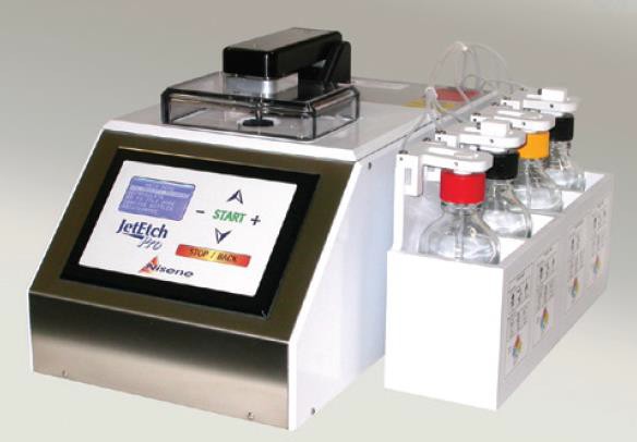
单粒子效应对应用于航天以及核工业的芯片往往造成极大危害,相对于传统的粒子***而言,利用脉冲激光进行检测可以极大地提***率,降低成本。以下型号型号激光SEE测试仪已经被应用于美国波音公司和NASA。

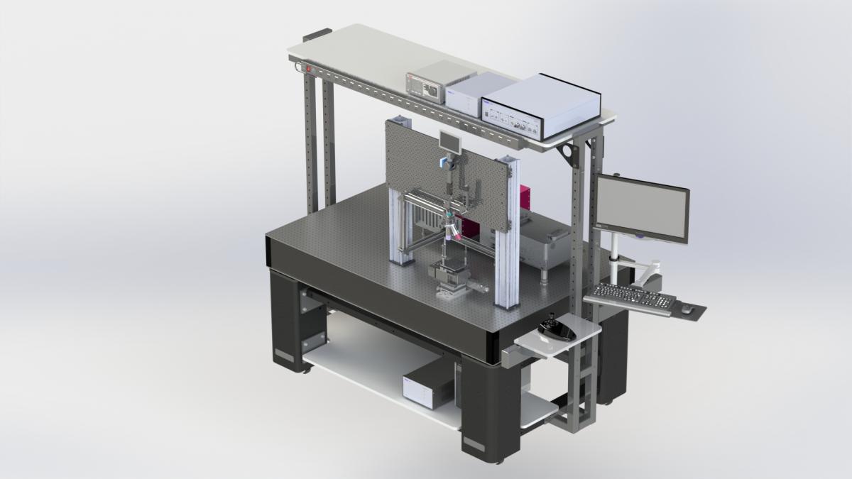
We offer custom SEE laser testing soluti***:
- Single photon
- Two phot***
- Selection of Pico and Femto second lasers
- Shortw***e 900nm to 1700nm and Visible imaging system
- Microscope objective choices; 200X, 100X, 50X 20X
Additional Features:
- High accuracy X-Y-Z motorized stages ( nm resolution) 50mm tr***el XYZ, 0.1micron resolution
- Joystick for X-Y
- Tilt stat ( 3 rotation axes) manual micrometer or motorized
- Protective enclosure
- Dual microscope objective top and bottom (optional)
- Replace Synchrotron beam-line time and high cost
- For space, military, aerospace, Railways, Automotive, ***ionic
Applicati***:
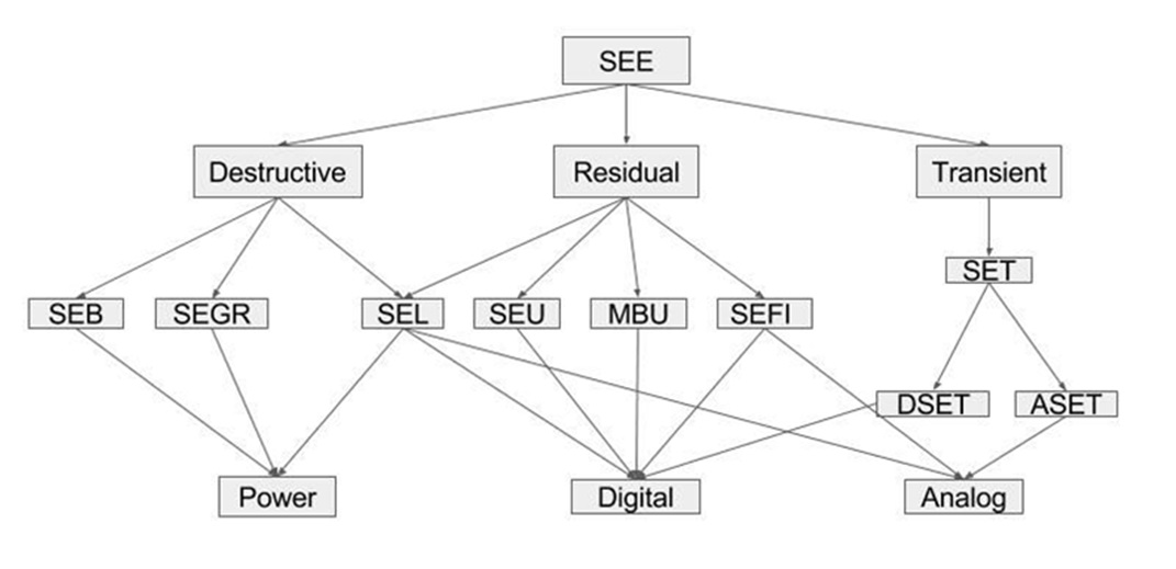
- SEU: Single Event Upset
- SET: Single Event Transient
- SEL: Single Event Latch-up
- SEGR: Single Event Gate Rupture
- SEB: Single Event Burnout
- SEGR: Single Event Gate Rupture
- SEFI: Single Event Functional Interrupt
Semiconductor Failures
The primary effects of natural space radiation on spacecraft electronics are total ionizing dose (TID) and single event effects (SEE). TID creates bulk-oxide and an interface-trap charge that reduces transistor gain and shifts the operating properties (e.g., threshold voltage) of semiconductor devices. TID accumulation will cause a device to fail if (1) the transistor threshold voltage shifts far enough to cause a circuit malfunction, (2) the device fails to operate at the required frequency, and/or (3) electrical isolation between devices is lost. SEE occurs when a co***ic ray or other very high-energy particle impinges on a device. The particle generates a dense track of electron-hole pairs as it passes through the semiconductor, and those free carriers are collected at doping juncti***. The net effect is that the circuit is perturbed and may lose data (called a single-event upset or SEU). The passage of a sufficiently energetic particle through a critical device region can even lead to permanent failure of an IC due to single-particle-event latchup (SEL), burnout, or dielectric/gate rupture. In general, components that exhibit SEL are not acceptable for space applicati*** unless the latchup can be detected and mitigated. Burnout and gate rupture are especially problematic for high-voltage and/or high-current electronics associated with space-borne power supplies. SEE h***e become an increasing concern as ICs begin to use ***aller device geometries and lower operating voltages, leading to reduced nodal capacitance and charge stored on circuit nodes. In addition to these primary effects, displacement damage effects caused by high-energy prot*** and electr*** can reduce mission lifetimes due to long-term damage to CCDs, optoelectronics, and solar cells.
|
What should I use for: |
He***y i*** |
Laser |
|
|
Single photon |
Two-photon |
||
|
Screening devices with different designs in the same technology node for SEU-MBU |
+ |
++ |
(+) |
|
Accurate SEU cross section vs LET measurement for a memory device |
++ |
|
|
|
Testing fault-tolerant system level soluti*** |
+ |
++ |
+ |
|
Analyzing deep charge collection mechani***s |
+ |
+ |
(++) |
|
Mapping SEL sensitive area of a flip-chip device |
|
+ |
++ |
|
Validating an SEL-free design |
++ |
+ |
|
|
Studying rare SEFI events in a recent digital devices |
|
++ |
++ |
|
Validating the radiation hardening efficiency of a design update |
+ |
++ |
+ |
|
Obtain 3D view of charge collection volumes |
|
|
++ |